1N5408 General Purpose Rectifier Diodes 5 Pieces

The 1N5408, an axial lead standard recovery rectifier. The 1N5400 series of diodes are known for higher-current in the range of 1 to 3 amps applications. These diodes are regularly accessible in the bigger DO-201AD axial package, suitable for high heat dissipation. They are fairly low-speed rectifier diodes, which are not that efficient for square wave of more than 15kHz. They are widely used in household appliances and are highly recommended for such use.

Included in this package: 5 Pieces of 1N5408 General Purpose Rectifier Diodes
NGN 450.00
Qty:  Add to Cart
Currently item(s) in cart.

1N5399 General Purpose Plastic Diodes 5 Pieces

The 1N5399 is a general purpose plastic diodes for use in general purpose applications like in  power supplies, inverters, converters, and freewheeling diodes application.

Included in this package: 5 pieces 1N5399 general purpose plastic diodes
NGN 200.00
Qty:  Add to Cart
Currently item(s) in cart.

1N5819 Schottky Diode 5 Pieces

This 1N5819 Schottky diode, also known as hot-carrier diode is a semiconductor diode made by the intersection of a semiconductor with a metal. It has a low forward voltage drop and a quick switching activity. The cat's-stubble locators utilized as a part of the beginning of remote and metal rectifiers utilized in early power applications can be viewed as primitive Schottky diodes.

At the point when adequate forward voltage is connected, a flow of current occurs in the forward direction. A silicon diode normally has a forward voltage of 600– 700 mV, while the Schottky's forward voltage is 150– 450 mV. This lower forward voltage of the Schottky permits higher speedy switching and better performance of the system in used.
NGN 200.00
Qty:  Add to Cart
Currently item(s) in cart.

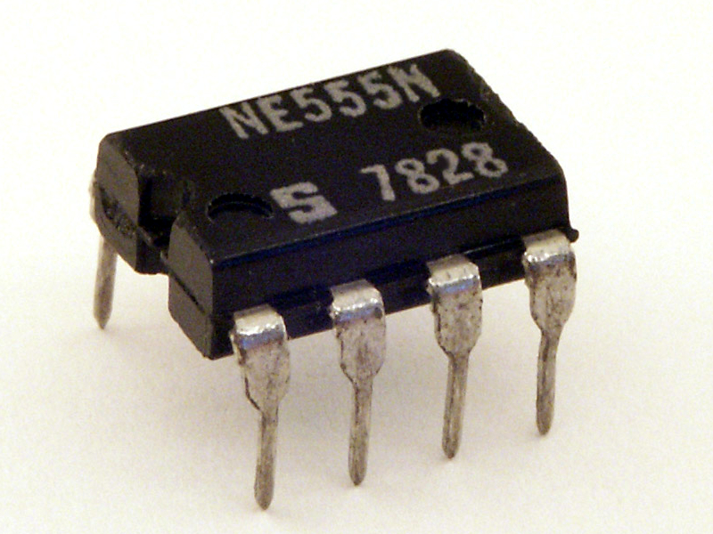
NE555 Integrated Circuit

The NE555 timer IC is an integrated circuit used in different applications such as timer circuit, pulse generation circuit and oscillator applications. The NE555 can be used to give time delays, as an oscillator, and as a flip-flop component. Subordinates give two (556) or four (558) timing circuits in one bundle.

Presented in 1972 by Signetics, the 555 is still in boundless use because of its low price, it's relatively easy to use, and strength. It is presently made by many electronics manufacturing companies in the first bipolar and in low-control CMOS. Starting at 2003, it was evaluated that 1 billion units were produced each year. The 555 is the most well known integrated circuit at any point made..
NGN 800.00
Qty:  Add to Cart
Currently item(s) in cart.


NE555 integrated circuit for timer ic, pulse generation circuits and oscillation circuit

The Part Name of 555 Timer IC

It has been erroneously assumed that the 555 got its name from the three 5 kω resistors utilized inside, however Hans Camenzind has expressed that the part number was subjective, in this way it's only a happenstance they coordinated. The "NE" and "SE" letters of the first parts numbers (NE555 and SE555) were temperature assignments for simple chips from Signetics, where "NE" was business temperature range and "SE" was military temperature range.

The Design of 555 Integrated Circuit

Contingent upon the maker, the standard 555 bundle incorporates 25 transistors, 2 diodes and 15 resistors on a silicon chip introduced in a 8-stick double in-line bundle (DIP-8). Other variations available include the 556 (a 14-stick DIP consolidating two 555s on one chip), and 558/559 (both a 16-stick DIP joining four decreased functionality timer chips on one chip).

The NE555 parts were business temperature range, 0 °C to +70 °C, and the SE555 part number assigned the military temperature range, −55 °C to +125 °C. These were accessible in both high-unwavering quality metal can (T bundle) and economical epoxy plastic (V bundle) bundles. Consequently the full part numbers were NE555V, NE555T, SE555V, and SE555T.

Low-control CMOS renditions of the 555 are likewise accessible, for example, the Intersil ICM7555 and Texas Instruments LMC555, TLC555, TLC551. CMOS timers utilize altogether less power than bipolar timers, likewise CMOS timers cause less supply noise than bipolar variation when the output switches states. The ICM7555 datasheet claims that it more often than not doesn't require a "control" capacitor and by and large does not require a decoupling capacitor over the power supply pins. For good plan rehearses, a decoupling capacitor ought to be incorporated, be that as it may, in light of the fact that noise delivered by the timer or change in power supply voltage may meddle with different parts of a circuit or impact its limit voltages.

Inside schematic of 555

The inside piece chart and schematic of the 555 timer are featured with a similar shading over every one of the three illustrations below to clear up how the chip is executed: 

Green: Between the positive supply voltage VCC and the ground GND is a voltage divider comprising of three indistinguishable resistors, which make two reference voltages at  1⁄3 VCC and  2⁄3 VCC. The last is associated with the control voltage pin. Each of the three resistors have a similar resistance, 5 kω for bipolar timers, 40 kω (or other higher resistance resistors) for CMOS timers. It is a false myth that the 555 IC got its name from these three 5 kω resistors. 
Internal block diagram of 555 integrated circuit
555 Internal Block Diagram


Yellow: The comparator negative input is associated with the higher-reference voltage divider of  2⁄3 VCC (and trigger pin), and comparator positive input is associated with the threshold pin. 

Orange: The comparator positive input is associated with the lower-reference voltage divider of  1⁄3 VCC, and comparator negative input is associated with the trigger pin. 

Purple: A SR flip-flop stores the condition of the timer and is controlled by the two comparators. The "Reset" pin supersedes the other two input pins, in this way the flip-flop(and consequently the whole timer) can be reset whenever needed. 

Pink: The output of the flip-flop is trailed by an output stage organize with push-pull (P.P.) input drivers that can supplu the "Output" pin with up to 200 mA (variations exist among different versions of 555). 

Cyan: Also, the output of the flip-flop turns on a transistor that interfaces the discharge pin to ground.
internal schematic of bipolar version of 555
555 Internal Schematic of Bipolar Version


Internal schematic of 555 cmos version
555 Internal Schematic of CMOS Version


Pin Out of 555


The table gives the detail of Pin Out of 555
555 Pin # 556 Pin # Pin Name Function of Pin
1 7 GND This is the ground pin. It is ground reference voltage (zero volts).
2 6,8 TRIGThis is the trigger pin, the OUT pin goes high and a timing interim begins when this input falls beneath  1⁄2 of CTRL voltage (ordinarily  1⁄3 VCC, CTRL being  2⁄3 VCC as a matter of course if CTRL is left open). All the more just, OUT will be high as long as the trigger is kept at low voltage. Output of the timer wholly relies on the amplitude of the supply trigger voltage connected to this pin.
3 5, 9OUT This is the output pin, the push-pull (P.P.) output is headed to GND or roughly 1.7 V beneath +VCC. (Note: CMOS timer parts can drive output up to VCC rail.) Signetics suggests a 1 nF decoupling capacitor be associated at the output pin in circuits that interface with digital logic inputs, which may help limit 555 output changing noise from causing issues.
4 4, 10 RESET This is the reset pin, a timing interim might be reset by driving this input to GND, yet the timing does not start again until the point when RESET transcends around 0.7 volts. 
5 3, 11 CTRL This is the control pin, the pin which gives control to the inside voltage divider (as a matter of course is  2⁄3 VCC). By applying a voltage to the Control Voltage input one can change the timing attributes of the 555. In many applications, this pin is however, not utilized, accordingly it is a good practice to connect a low-noise 10 nF decoupling capacitor (film or ceramic capacitor) between Control pin and Ground pin to remove the noise on the higher reference voltage. The control pin input can be utilized to construct an astable multivibrator with a modulated frequency output.
6 2, 12THR This is the threshold pin, the timing (OUT high) interval ends when the voltage at THR ("threshold") is greater than that at CTRL ( 2⁄3 VCC if CTRL is open). Overrides TRIG on the LM555.
7 1, 13 DIS This is the discharge pin. It is an  open-collector output, which may discharge a capacitor between intervals. In phase with output.
8 14 Vcc This is the positive supply rail pin. The usual range of voltage of bipolar parts are ordinarily 4.5 volt to 15 volts (a few of them rated up to 16 volts or 18 volts), however most bipolar parts will work at voltages as low as 3 volts. (Note: CMOS timer parts have a lower minimum voltage rating.) It is prescribed that a 100 nF decoupling capacitor be associated as close as conceivable to this pin, and alternatively a 10 to 100 uF storage capacitor depending on what is connected to the output pin. These capacitance ratings are a beginning point of consideration rather than obligatory ratings that must be utilized.

Modes of Operation of 555


The IC 555 has three working modes: 

Astable (free-running) mode: the 555 can work as an electronic oscillator. This has applications in LED and light flashers, generation of pulses, logic clocks, generation of tone in musical instruments, security alarms, modulation of pulse position et cetera. The 555 can be utilized as a basic ADC, changing analog value to a pulse length (e.g., choosing a thermistor as timing resistor permits the utilization of the 555 out of a temperature sensor and the time of the output pulse is controlled by the temperature). The utilization of a chip based circuit would then be able to change over the pulse time frame to temperature, linearize it and even give alignment means. 

Monostable mode: in this mode, the 555 is used as a "one-shot" pulse generator. This mode find uses in timers, detection of missing pulse, bounce-free switches, touch switches, frequency divider, capacitance estimation, pulse width regulation (PWM) et cetera. 

Bistable (schmitt trigger) mode: the 555 can work as a flip-flop, if the DIS pin is not connected and no capacitor is utilized. In this mode, it is used in bounce free switches.

1N4007 Rectifier Diodes

A diode allows electrical current to flow only in one direction. The 1N4001 group (or 1N4000 series is a group of well known 1 A (ampere) diodes universally useful silicon rectifier diodes, normally used as a part of AC adapters for normal household appliances. Blocking voltage may be from 50 to 1000 volts. This diode group is accessible in DO-41 axial package, SMA and MELF surface mount bundles.


NGN 600.00
Qty:  Add to Cart
Currently item(s) in cart.


Features of 1N4007


  • Low forward voltage drop
  • Low leakage current
  • High forward surge capability
  • Solder dip 275 °C max. 10 s, per JESD 22-B106
  • Compliant to RoHS Directive 2002/95/EC and in accordance to WEEE 2002/96/EC


Common Applications of 1N4007


For use in general purpose rectification of power supplies, inverters, converters and freewheeling diodes application.

Note: These devices are not AEC-Q101 qualified.

Mechanical Data


Case: DO-204AL, molded epoxy body. Molding compound meets UL 94 V-0 flammability rating. Base P/N-E3 - RoHS compliant, commercial grade. The terminal pins are Matte tin plated leads, solderable per J-STD-002 and JESD 22-B102. E3 suffix meets JESD 201 class 1A whisker test
As for the polarity, the color band denotes cathode end, while the other end is the anode.

To learn more get the data sheet here.

1N4148 Signal Diode

The 1N4148 is a standard silicon switching signal diode. It stands out amongst the most well known and enduring switching diodes as a result of its dependable features and it's inexpensive. Its name comes from the JEDEC classification. The 1N4148 is helpful in switching applications up to around 100 MHz with an invert recuperation time of close to 4 ns.

As one of the most well-known mass-produced switching diode, the 1N4148 supplanted the older version, the 1N914. A major difference between them is in their leakage current rating at 25°C: 25 nA @ - 20V versus 5 µA @ - 75V, with greatest leakage for both at 150°C to be 50 µA @ - 20V. Today makers create the 1N4148 and offer it as either part number. It was second-sourced by numerous producers; Texas Instruments recorded their model of the diode in an October 1966 information sheet. These types of diodes have a persisting ubiquity in low-current applications.[4][5]

Despite the fact that the first 1N4148 and 1N914 existed just in a pivotal bundle, the 1N4148 was later repackaged into different surface-mount bundles.
750.00
Qty:  Add to Cart
Currently item(s) in cart.

1N4148 signal diode fast switching signal diode

Specifications


  • IFSM = 1.0 A (pulse width = 1 s), 4.0 A (pulse width = 1 µs) — non-repetitive peak forward surge 
  • VRRM = 75-100 V — maximum repetitive reverse voltage
  • IF = 200-300 mA — maximum direct forward current
  • VF = 1.0 V at 10 mA current
  • IO = 75-200 mA — average rectified forward current
  • TRR < 4 ns — reverse-recovery time
  • PD = 500 mW — power dissipation


4.7K Rotary Wire Wound Potentiometer

A rotary wire wound potentiometer can open up many fascinating UIs. Turn the pot and the resistance changes. When the Vcc is connected to the outer pin and the ground (GND) pin is connected to the other, the pin in the middle will have a voltage that changes from 0 to VCC contingent upon the rotation of the pot. You get a variable input from when the center pin is connected to an ADCon a microcontroller.

The diameter of the pot is about 1/4" and a linear taper of 4.7k also written as 4k7. This pot has a ¼" mounting measurement and has a 4.7K direct decrease. Check the datasheet for dimensional illustrations and for other useful information.
NGN 550.00
Qty:  Add to Cart
Currently item(s) in cart.


Specifications

Resistance: 4.7K-Ohms
Resistance tolerance: 5%
Rated Power: 1.0 Watt
Technology: Wire wound potentiometer
Sliding Noise: less Than 47millivolt (mV)
Total Rotation: 300° +/- 5°

LM317T Voltage Regulator 2 Pieces

The LM317 is one of the most popular positive linear voltage regulator. It was invented by Robert C Dobkin in 1976 at the time he was working at National Semiconductor.

The negative complement of LM317 is the LM337 which regulates voltages below the reference voltage, rather than above.
NGN995.00
Qty:  Add to Cart
Currently item(s) in cart.

Bundles of LM317 for sale in Nigeria
Pin-out configuration of LM317
Typical schematic diagram for LM317.
schematic for a constant current source with output voltage of 0 - 1.8

The LM317 can output a voltage from 1.25 to 37. As can be seen from the schematic diagram, the output voltage is determined by the values of the two resistors connected between the Vout and ADJ pins, i.e. RH and RL.

Specifications of LM317

Symbol Parameter Value
Vout
1.25 - 37 V
Vin - Vout  difference 30 - 40 V
Tj operating junction temperature  0 - 125 degree Celsius
Io (max) maximum output current 1.5 Amperes
IL (min) minimum load current typically, 3.5mA with a maximum of 12mA
PD power dissipation  internally limited
R⬲JA thermal resistance of junction to ambient 80 degree Celsius/W
R⬲JC thermal resistance of junction to case 5 degree Celsius/W

If the device is not mounted on a heat sink and there is a surrounding temperature of about 50 ⁰C, for example, on a hot summer day inside a container, a most extreme power dissipation of (TJ-TA)/RθJA = ((125-50)/80) = 0.98 W can be allowed. (A bit of gleaming sheet metal of Aluminum with the measurements 6 x 6 cm and 1.5 mm thick, brings about a thermal resistance that grants 4.7 W of heat dissipation. 

When operating in a constant voltage mode with an input voltage source, VIN at 34 V with a desired output voltage of 5 V, the highest output current will be PMAX/(VI-VO) = 0.98/(34-5) = 32 mA. 

For a constant current mode with an input voltage source, VIN at 12 V and a forward voltage drop of VF=3.6 V, the highest output current will be PMAX/(VI - VF) = 0.98/(12-3.6) = 112 mA.

LM317 Operation

As direct controllers, the LM317 and LM337 are utilized as a part of DC to DC converter applications.

All linear regulators normally waste power, the power wasted is the product of the current and the voltage difference between input and output. When in use LM317 ordinarily requires a heat sink to prevent the working temperature going too high. For large voltage differnces, the wasted energy in the form of heat can be more than that supplied to the circuit. This is what you'll sacrifice for using linear regulators which are a basic approach to supply a steady voltage with couple of extra parts. A better way is to use a switching voltage regulator which usually performs better, however has a bigger impression and requires many other related components.

For LM317 with heat dissipating mounting tab, for example, TO-220, the tab is hooked up inside to the output pin which is the reason why it may be necessary to isolate the tab or the heat sink from different parts of the application circuit. Inability to do this may make the circuit short.

IRF540 TO-220 100V 33A Power MOSFET transistor N channel 3 Pieces

These are N-Channel improvement mode silicon gate power metal oxide semi-conductor field effect (MOSFET) transistors. They are advanced power MOSFETs composed, tried, and ensured to withstand an indicated level of energy in the breakdown slide mode of operation. These power MOSFETs are intended for applications, for example, switching regulators, switching converters, DC motors drivers, relay drivers, and drivers for high power bipolar switching transistors requiring fast and low gate drive power. These sorts can be worked straightforwardly from incorporated circuits.

NGN660.00
Qty:  Add to Cart
Currently item(s) in cart.


Included In The Package

3 Pieces of IRF540 TO-220 100V 33A Power MOSFET

Features IRF540 TO-220 100V 33A Power MOSFET transistor


  • 25A and 28A, 80V and 100V
  • rDS(ON) = 0.077Ω and 0.100Ω
  • Single Pulse Avalanche Energy Rated
  • Nanosecond Switching Speeds
  • Linear Transfer Characteristics
  • High Input Impedance
  • Related Literature
  • TB334 “Guidelines for Soldering Surface Mount
  • Components to PC Boards”
For more information, get the datasheet here.
The metal– oxide– semiconductor field-effect transistor (MOSFET, MOS-FET, or MOS FET) is a sort of field-effect transistor (FET). It has an insulated gate, whose voltage decides the conductivity of the gadget. This capacity to change conductivity with the measure of connected voltage can be utilized to amplify or switching electronic signals. A metal-oxide semiconductor field-effect transistor or MISFET is a term practically synonymous with MOSFET. Another equivalent word is IGFET which stands for insulated gate field-effect transistor. 

The fundamental preferred standpoint of a MOSFET is that it requires close to no input current to control the current drawn by the load, in comparison with bipolar transistors. In an "improvement mode" MOSFET, voltage connected to the gate terminal leads to an increase in the conductivity of the gadget. When the device is in "depletion mode", voltage connected to the gate lessens the conductivity.

The "metal" in the name MOSFET is presently frequently a misnomer on the grounds that the gate material is usually a layer of polysilicon (polycrystalline silicon). "Oxide" in the name can likewise be a misnomer, as various dielectric materials are utilized with the point of acquiring solid channels with least connected voltages. The MOSFET is by a long shot the most widely recognized transistor in computerized circuits, as several thousands or a great many of them might be incorporated into a memory chip or microchip. Since MOSFETs can be made with either p-sort or n-sort semiconductors, reciprocal sets of MOS transistors can be utilized to make switching circuits with low power utilization, as CMOS rationale.

103 10K ohm Top regulation Multiturn Trimmer Potentiometer 5 pieces

This is a 3296W-1-103LF, 3296W, 103 or 10K ohm Top regulation Multiturn Trimmer Potentiometer High Precision Variable Resistor

A potentiometer is a three-terminal resistor with a sliding or turning contact that forms a variable voltage divider. If just two terminals are utilized, one end and the wiper, it functions as a variable resistor or rheostat.

The measuring instrument called a potentiometer is basically a voltage divider utilized for measuring electric potential (voltage); the segment is an execution of a similar guideline, subsequently its name.

Potentiometers are usually used to control electrical gadgets, for example, volume controls on sound hardware. Potentiometers worked by a system can be utilized as position transducers, for instance, in a joystick. Potentiometers are once in a while used to specifically control critical power (more than a watt), since the power through the potentiometer would be practically identical to the power in the controlled load.

This package contains 5 pieces of the potentiometers.

NGN650.00
Qty:  Add to Cart
Currently item(s) in cart.


Features of 103 10K ohm Multiturn Trimmer Potentiometer


  • Brand Name:IGMOPNRQ
  • Condition:New
  • Technology:Wirewound
  • Model Number:3296W-1-103LF
  • Type:Metallic Glass Glaze Potentiometer
  • Resistance:10,000 ohm (10k ohm)
  • Resistance Tolerance:±10%
  • Rated Power:0.5W, 1/2W
  • Maximum Operating Voltage:500V
  • Operating Temperature:-55 °C to +150 °C

LM358 LM358P DIP-8 Operational Amplifiers 5 pieces

Using the circuit plans consummated for quad operational amplifiers, this double operation amp includes low power drain, a typical mode input voltage range stretching out to ground/VEE, and single supply or split supply operation. The LM358 model is comparable to one-portion of a LM324.

These devices have some advantages over standard operational amps in single supply applications. They can work at supply voltages as low as 3.0 V or as high as 32 V, with quiescent current around one-fifth of those related with the MC1741 (on a for every amp premise). The basic mode input range incorporates the negative supply, accordingly eliminating the need for outer biasing parts in numerous applications. The output voltage range likewise incorporates the negative power supply voltage.

The LM358 series is made using two internally compensated, two−stage operational amplifiers. The first stage of each consists of differential input devices Q20 and Q18 with input buffer transistors Q21 and Q17 and the differential to single ended converter Q3 and Q4. The first stage performs not only the first stage gain function but also performs the level shifting and transconductance reduction functions. By reducing the transconductance, a smaller compensation capacitor (only 5.0 pF) can be employed, thus saving chip area.

The transconductance reduction is accomplished by splitting the collectors of Q20 and Q18. Another feature of this input stage is that the input common mode range can include the negative supply or ground, in single supply operation, without saturating either the input devices or the differential to single−ended converter. The second stage consists of a standard current source load amplifier stage. Each amplifier is biased from an internal−voltage regulator which has a low temperature coefficient thus giving each amplifier good temperature characteristics as well as excellent power supply rejection.

This package include 5 pieces of LM358
NGN577.00
Qty:  Add to Cart
Currently item(s) in cart.

LM358-LOW-POWER-DUAL-OPERATIONAL-AMPLIFIERS-LM358N-Amplifier-DIP8-LM358P

Highlights of the LM358 LM358P DIP-8 Operational Amplifiers


  • Short out Protected Outputs 
  • Genuine Differential Input Stage 
  • Single Supply Operation: 3.0 V to 32 V 
  • Low Input Bias Currents 
  • Inside Compensated 
  • Regular Mode Range Extends to Negative Supply 
  • Single and Split Supply Operation 
  • ESD Clamps on the Inputs Increase Ruggedness of the Device without Affecting Operation 
  • Pb-Free Packages are Available

Learn more about the product here or get the datasheet.

IRFZ44N or IRFZ44NPBF POWER MOSFET 5 Pieces

This is IRFZ44N, or simply IRFZ44 or better still IRFZ44NPBF POWER MOSFET with a voltage of 55V or maximum current of 41A and a resistance of 17.5megaOhm 42nC in a TO-220 package. The power dissipation, supply voltage and operating temperature all meet international standards.

This Power MOSFETs utilize advanced processing techniques to achieve extremely low on-resistance per silicon area. This benefit, combined with the fast switching speed and rugged-packaged
device design that IGMOPNRQ power MOSFETs are well known for, provides the designer with an extremely efficient and reliable device for use in a wide variety of applications. The TO-220 package is universally preferred for all commercial-industrial applications at power dissipation levels to approximately 50 watts. The low thermal resistance and low package cost of the TO-220 contribute
to its wide acceptance throughout the industry.

This package contains 5 pieces of IRFZ44N

NGN 1,155.00
Qty:  Add to Cart
Currently item(s) in cart.


Features of IRFZ44N or IRFZ44NPBF POWER MOSFET


  • Continuous Drain Current (Id): 41 A
  • Drain-Source Breakdown Voltage (Vds): 55 V
  • Drain-Source Resistance (Rds): 23 mOhms
  • Transistor Polarity: N-Channel
  • Operating Junction and Storage Temperature Range: - 55 to + 175oC
  • Gate-Source Breakdown Voltage (Vgs): 20 V
  • Gate Charge (Qg): 42 nC
  • Power Dissipation (Pd): 83 W
  • Mounting Style: Through Hole
  • Package / Case: TO-220-3
  • Model Number: IRFZ44N
  • Packaging: Tube
  • Model Name: IGMOPNRQ

To learn more, get the datasheet.


5mm Assorted LED Kit of DIY Electronic Projects

This is a 5mm, five (5) different colors of LED (Light Emitting Diode).  An assorted kit for DIY LED's related or electronic project. This set is made up of five (5) different colors of LED i.e. White, Yellow, Red, Green and Blue for different electronic diy projects.

Different colors of LED have different voltage and current ratings. Check the breakdown of the different colors available in this offer and the respective voltage and current rating below.

NGN 691.00
Qty:  Add to Cart
Currently item(s) in cart.


Included in the package are:

50pieces LED Assorted Kit

  • White    5mm   10pcs    3V-3.2V 20mA
  • Red      5mm   10pcs    1.8V-2V 20mA
  • Greem    5mm   10pcs   1.8V-2V 20mA
  • Yellow   5mm   10pcs    2V-2.3V 20mA
  • Blue     5mm   10pcs    3 V-3.2V 20mA
  1. Most Recent

Search Here

Follow Us