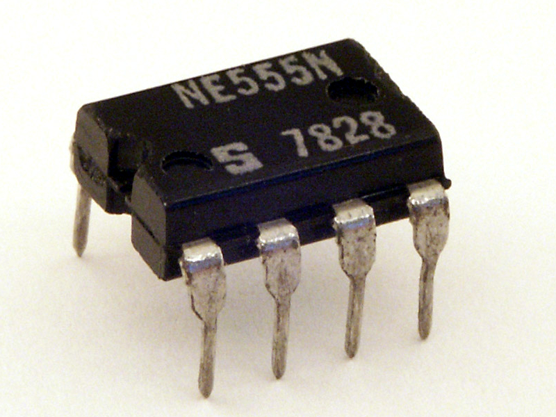
The NE555 timer IC is an integrated circuit used in different applications such as timer circuit, pulse generation circuit and oscillator applications. The NE555 can be used to give time delays, as an oscillator, and as a flip-flop component. Subordinates give two (556) or four (558) timing circuits in one bundle.
Presented in 1972 by Signetics, the 555 is still in boundless use because of its low price, it's relatively easy to use, and strength. It is presently made by many electronics manufacturing companies in the first bipolar and in low-control CMOS. Starting at 2003, it was evaluated that 1 billion units were produced each year. The 555 is the most well known integrated circuit at any point made..
The Part Name of 555 Timer IC
It has been erroneously assumed that the 555 got its name from the three 5 kω resistors utilized inside, however Hans Camenzind has expressed that the part number was subjective, in this way it's only a happenstance they coordinated. The "NE" and "SE" letters of the first parts numbers (NE555 and SE555) were temperature assignments for simple chips from Signetics, where "NE" was business temperature range and "SE" was military temperature range.
The Design of 555 Integrated Circuit
Contingent upon the maker, the standard 555 bundle incorporates 25 transistors, 2 diodes and 15 resistors on a silicon chip introduced in a 8-stick double in-line bundle (DIP-8). Other variations available include the 556 (a 14-stick DIP consolidating two 555s on one chip), and 558/559 (both a 16-stick DIP joining four decreased functionality timer chips on one chip).
The NE555 parts were business temperature range, 0 °C to +70 °C, and the SE555 part number assigned the military temperature range, −55 °C to +125 °C. These were accessible in both high-unwavering quality metal can (T bundle) and economical epoxy plastic (V bundle) bundles. Consequently the full part numbers were NE555V, NE555T, SE555V, and SE555T.
Low-control CMOS renditions of the 555 are likewise accessible, for example, the Intersil ICM7555 and Texas Instruments LMC555, TLC555, TLC551. CMOS timers utilize altogether less power than bipolar timers, likewise CMOS timers cause less supply noise than bipolar variation when the output switches states. The ICM7555 datasheet claims that it more often than not doesn't require a "control" capacitor and by and large does not require a decoupling capacitor over the power supply pins. For good plan rehearses, a decoupling capacitor ought to be incorporated, be that as it may, in light of the fact that noise delivered by the timer or change in power supply voltage may meddle with different parts of a circuit or impact its limit voltages.
Inside schematic of 555
The inside piece chart and schematic of the 555 timer are featured with a similar shading over every one of the three illustrations below to clear up how the chip is executed:
Green: Between the positive supply voltage VCC and the ground GND is a voltage divider comprising of three indistinguishable resistors, which make two reference voltages at 1⁄3 VCC and 2⁄3 VCC. The last is associated with the control voltage pin. Each of the three resistors have a similar resistance, 5 kω for bipolar timers, 40 kω (or other higher resistance resistors) for CMOS timers. It is a false myth that the 555 IC got its name from these three 5 kω resistors.
 |
| 555 Internal Block Diagram |
Yellow: The comparator negative input is associated with the higher-reference voltage divider of 2⁄3 VCC (and trigger pin), and comparator positive input is associated with the threshold pin.
Orange: The comparator positive input is associated with the lower-reference voltage divider of 1⁄3 VCC, and comparator negative input is associated with the trigger pin.
Purple: A SR flip-flop stores the condition of the timer and is controlled by the two comparators. The "Reset" pin supersedes the other two input pins, in this way the flip-flop(and consequently the whole timer) can be reset whenever needed.
Pink: The output of the flip-flop is trailed by an output stage organize with push-pull (P.P.) input drivers that can supplu the "Output" pin with up to 200 mA (variations exist among different versions of 555).
Cyan: Also, the output of the flip-flop turns on a transistor that interfaces the discharge pin to ground.
 |
| 555 Internal Schematic of Bipolar Version |
 |
| 555 Internal Schematic of CMOS Version |
Pin Out of 555
The table gives the detail of Pin Out of 555
| 555 Pin # |
556 Pin # |
Pin Name |
Function of Pin |
| 1 |
7 |
GND |
This is the ground pin. It is ground reference voltage (zero volts). |
| 2 |
6,8 |
TRIG | This is the trigger pin, the OUT pin goes high and a timing interim begins when this input falls beneath 1⁄2 of CTRL voltage (ordinarily 1⁄3 VCC, CTRL being 2⁄3 VCC as a matter of course if CTRL is left open). All the more just, OUT will be high as long as the trigger is kept at low voltage. Output of the timer wholly relies on the amplitude of the supply trigger voltage connected to this pin. |
| 3 |
5, 9 | OUT |
This is the output pin, the push-pull (P.P.) output is headed to GND or roughly 1.7 V beneath +VCC. (Note: CMOS timer parts can drive output up to VCC rail.) Signetics suggests a 1 nF decoupling capacitor be associated at the output pin in circuits that interface with digital logic inputs, which may help limit 555 output changing noise from causing issues. |
| 4 |
4, 10 |
RESET |
This is the reset pin, a timing interim might be reset by driving this input to GND, yet the timing does not start again until the point when RESET transcends around 0.7 volts. |
| 5 |
3, 11 |
CTRL |
This is the control pin, the pin which gives control to the inside voltage divider (as a matter of course is 2⁄3 VCC). By applying a voltage to the Control Voltage input one can change the timing attributes of the 555. In many applications, this pin is however, not utilized, accordingly it is a good practice to connect a low-noise 10 nF decoupling capacitor (film or ceramic capacitor) between Control pin and Ground pin to remove the noise on the higher reference voltage. The control pin input can be utilized to construct an astable multivibrator with a modulated frequency output. |
| 6 |
2, 12 | THR |
This is the threshold pin, the timing (OUT high) interval ends when the voltage at THR ("threshold") is greater than that at CTRL ( 2⁄3 VCC if CTRL is open). Overrides TRIG on the LM555. |
| 7 |
1, 13 |
DIS |
This is the discharge pin. It is an open-collector output, which may discharge a capacitor between intervals. In phase with output. |
| 8 |
14 |
Vcc |
This is the positive supply rail pin. The usual range of voltage of bipolar parts are ordinarily 4.5 volt to 15 volts (a few of them rated up to 16 volts or 18 volts), however most bipolar parts will work at voltages as low as 3 volts. (Note: CMOS timer parts have a lower minimum voltage rating.) It is prescribed that a 100 nF decoupling capacitor be associated as close as conceivable to this pin, and alternatively a 10 to 100 uF storage capacitor depending on what is connected to the output pin. These capacitance ratings are a beginning point of consideration rather than obligatory ratings that must be utilized. |

Modes of Operation of 555
The IC 555 has three working modes:
Astable (free-running) mode: the 555 can work as an electronic oscillator. This has applications in LED and light flashers, generation of pulses, logic clocks, generation of tone in musical instruments, security alarms, modulation of pulse position et cetera. The 555 can be utilized as a basic ADC, changing analog value to a pulse length (e.g., choosing a thermistor as timing resistor permits the utilization of the 555 out of a temperature sensor and the time of the output pulse is controlled by the temperature). The utilization of a chip based circuit would then be able to change over the pulse time frame to temperature, linearize it and even give alignment means.
Monostable mode: in this mode, the 555 is used as a "one-shot" pulse generator. This mode find uses in timers, detection of missing pulse, bounce-free switches, touch switches, frequency divider, capacitance estimation, pulse width regulation (PWM) et cetera.
Bistable (schmitt trigger) mode: the 555 can work as a flip-flop, if the DIS pin is not connected and no capacitor is utilized. In this mode, it is used in bounce free switches.

|


0 Reviews:
Post a Comment